It is the first member of thyristor family devices and it is named after the inventor William Bradford Shockley. Once we understand this basic operation of this diode, we will easily understand the next concepts covered in thyristors. Let us know about the Shockley diode working and applications.
Introduction to Shockley Diode
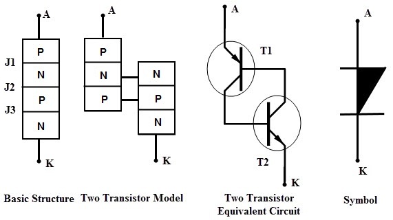
The Shockley diode or PNPN diode is a four layer (P-N-P-N), two terminals (namely anode and cathode) semiconductor switching device. It is also called as four layer diode. It functions like a normal diode without any trigger inputs, in reverse biased condition, no current flows through it and in forward biased condition current flows through it when the voltage across it is more than the break over voltage of it. These diodes have only two states, either ON or OFF that’s why these are classified as a thyristors. The basic construction, two transistor analogy and symbol of the shockley diode are shown in below figure.
The construction of this diode is simple: it is constructed by joining the four layers to form PNPN junction. The equivalent circuit of this diode using two transistors is shown in above figure where in the collector of a transistor T1 is connected to the base of T2. The junction J1 is formed at the emitter base junction of T1, J2 is at common connected base collector junction between T1 and T2, and the J3 is at base emitter junction of T2. Therefore, as the base emitter junctions, J1 and J3 must be forward biased and as a collector base junction, J2 must be reverse biased for linear operation. Back to top
Working
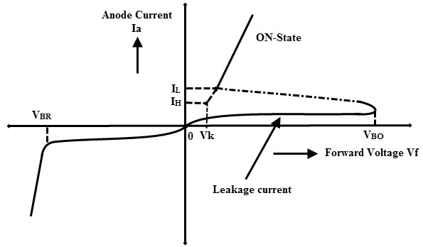
As discussed above, the these diodes consists of three junctions J1, J2 and J3. When the voltage is applied to the this diode in such a way that anode is made positive with respect to cathode, junctions J1 and J3 are forward biased and J2 is reverse biased. Until the voltage across the diode is less than the break over voltage, as an open switch this diode exhibits a very high resistance and allows no current to flow through it. Once the break over voltage is reached (as the forward voltage is increased), it exhibits a very low resistance due to the breakdown of junction J2. Therefore, it acts like a short circuit and allows the current to flow until the current reaches to the holding current level of the diode. This forward current flow through the diode is depends on the voltage applied and the external load resistance. The below figure shows the VI characteristics of shockley diode for conducting and non conducting states where ON-state current flows only when the voltage is more than the break over voltage VBO.
When the anode is made negative with respect to the cathode, junctions J1 and J3 are reverse biased and junction J2 is forward biased. If the reverse bias voltage is increased (beyond the breakdown voltage of the shockley diode), J1 and J3 are reverse biased, then the reverse current will flow through the diode as shown in above figure. This reverse current produces the heat, further this could ruin the entire diode. Therefore, shockley diode should never be operated in reverse biased condition with a voltage equal to the reverse breakdown voltage. Once the shockley diode is ON it acts like a closed switch offer a very low resistance to the current flow. To turn OFF the diode (or to act like an open switch), the applied voltage must be reduced to a value such that current flowing through the diode is less than the holding current IH of the diode. In this state, junction J2 comes from reverse breakdown state and restores its high resistance value. Back to top
Shockley Diode Applications
Shockley diodes are used mainly for switching applications. The two main important applications of shockley diode as relaxation oscillator and trigger switch are discussed below.
As Relaxation Oscillator
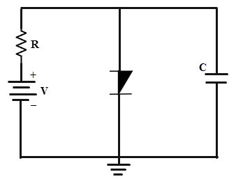
The below figure shows the relaxation oscillator circuit using a shockley diode. In this the diode is connected across the capacitor power with a power supply battery.
When the battery voltage is applied to the circuit, the capacitor charges through a resistance R. When the applied voltage or voltage across the capacitor is more than the break over voltage of shockley diode, it becomes turned ON and acts as a Switch. This causes rapidly to discharge the capacitor through the diode. And when the current through the diode is less than the holding current of the diode, the diode becomes turned OFF and capacitor charges again. The voltage across the capacitor is shown below figure where the voltage at the reference is more than zero volts because the capacitor will not discharge completely.
Back to top
As Trigger Switch
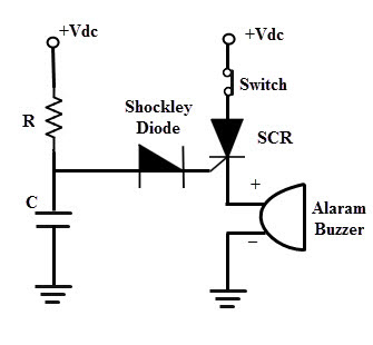
Most common applications of Shockley diode are switching circuits , to turn ON the SCR. In the below circuit SCR is triggered by the shockley diode. The Resistive and capacitor RC network is fed with a DC supply which drives the shockley diode.
When the VDC is applied, shockley is forward biased and also capacitor starts charging through the resistance. When the charging voltage of the capacitor reaches to the break over voltage of the diode, diode starts conducting and the capacitor starts discharging through the diode. This conduction of shockley diode drives the SCR into turn ON state, then the buzzer gives an alarm. Once the SCR is turned ON it will remain in the latching or ON state until the power is removed or commutation techniques applied to SCR. So there is no effect of the gate or shockley diode circuit to make SCR OFF. However the triggering times of SCR is controlled by selecting proper values of capacitor and resistors. Back to top Comment * Name * Email * Website
Δ


![]()