MEMS refers to the devices that have the characteristics of very small in size raging from a few micrometers to millimetre which combine both mechanical and electrical components and that are fabricated using integrated circuit batch processing technologies. MEMS devices are able to sense, control and actuate on the micro scale and also produce the outcome on the micro scale. Generally, the size of these devices is the range of 20 micrometers to a millimetre. MEMS devices are found in a variety of applications including industrial, automotive, instrumentation, defence and medical fields.
What is MEMS Technology?
MEMS stands for Microelectromechanicalsystems, is a technology used for the microfabrication of electrical and mechanical components on a single wafer. This term is originated in the United States in 1990s, also referred as micro systems in Europe and labelled as micro machines in Japan. Prior to this technology was referred as silicon micro machining. MEMS technology provides a new functionality that previously could not be offered by the semiconductor devices.
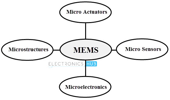
In other words MEMS is a precision device in which mechanical parts and micro sensors along with the signal conditioning circuits are fabricated on a small piece of silicon. The letter S in the MEMS acronym indicates the systems which reflect that this technology contributes the creation of new system solutions. The elements that are integrated on the silicon chip using MEMS technology include micro sensors, mechanical structures, microelectronics and micro actuators as shown in figure. Micro sensors detects the changes of the system’s environment by measuring thermal, chemical, electromagnetic, mechanical information, whereas these physical variables are processed by Microelectronics and then Micro actuators acts according to the changes of the environment.
Some of the main factors that results a high level of interest in MEMS technology are Due to the pure crystalline structure with a silicon content of 99.999 percent, MEMS devices gives excellent mechanical characteristics which are resulting in no mechanical hysteresis or material fatigue. It is possible to produce low cost and high-volume MSME devices with batch wafer processing technology. This high-volume production is very convenient with availability of cutting edge IC processing equipments. A lateral dimension to sub micron level is greatly controlled. Availability of sophisticated devices for test and diagnosis and also high end software systems are available for design and simulation. In the business side, MEMS devices assure large financial gains to the multiple emerging markets. MSME is selected as one of the three technologies expected to increase the growth of the economy in the 21st century by the Business Week in 1999.
MEMS Technology Fabrication
MEMS progress is resulted from a logical step in the silicon revolution and later with addition of micro machines allowed the integration of electronics with mechanical components to produce high performance, low cost and high functionality integrated micro systems. Silicon is the perfect material for fabricating micro sensors and micro actuators for different range of applications because it is a well-characterized material having properties like high thermal conductivity, lack of hysteresis, low bulk expansion, well-defined electrical properties with sensitive to strain, temperature, stress and other environmental factors, similar modulus of elasticity to that of steel, etc. In MEMS fabrication, silicon can be chemically etched into various shapes and associated thin-film materials such as poly silicon , aluminium and silicon nitride can be micro machined in batches into a vast variety of mechanical shapes and configurations. Various technologies are available for MEMS fabrication, two major technologies are usually employed are bulk micro machining and surface micro machining. Let us discuss in brief about these two.
Bulk Micro machining
It is the oldest and most popular technology used in the MEMS fabrication. In this, mechanical structures are created within the boundaries of single-crystal silicon wafer by selectively removing parts of a wafer material by using orientation-dependant etching. Based on the phase of etchant, bulk micro machining fabrication can be divided into wet etching and dry etching. In wet etching, the material is removed by immersing a silicon wafer in liquids etchants that relying on aqueous chemicals. The etching (removing of wafer material) can be either anisotropic, isotropic, or a combination of both. In isotropic etching, silicon wafer is removed in all the directions independently according to the crystallographic orientation of the substrate. In this, accuracy of structure definition is not very good but depends on the factors like temperature, etchant concentration and time. HNA is the most common form of silicon etches which comprises of the combination of nitric acid (HNO3), hydrofluoric acid (HF) and acetic acid (CH3CHOOH). These types of etchants are limited by the geometric structure to be etched. Etch rate can slow down and in case of deep and narrow channels this rate can stop due to diffusion limiting factors. However, this can be minimized by agitation of the etchant, resulting in structures with near perfect and rounded surfaces as shown in below figure.
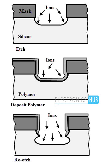
In anisotropic etching, etch rate depends on the crystallographic orientation of the wafer. The most common anisotropic etchant is potassium hydroxide (KOH) which is relatively safe to use. This anisotropic etches are progressing rapidly in the crystal direction perpendicular to the 110 plane and less rapidly in the direction perpendicular to the 100 plane. The above figures C and D show the examples of anisotropic etching. Dry etching relies on plasma and vapour based methods of etching using suitably reactive vapours or gases usually at high temperatures. Reactive Ion Etching (RIE) is the most common for MEMS that utilizes the additional energy in the form of RF (Radio Frequency) power to drive the chemical reaction. The etching can occur at much lower frequencies typically in the range 150 to 250 degree centigrade because energetic ions are accelerated towards the material to be etched within the plasma phase supplying the additional energy needed for the reaction. The deep trenches and pits, or arbitrary shapes with vertical walls can be etched due to the reason that the RIE is not limited by the crystal planes in the silicon. Deep Reactive Ion Etching (DRIE) is a much higher-aspect-ratio method that involves an alternative process of high density of plasma etching and protective polymer deposition to achieve greater aspect ratios as shown in figure.
Etch –stopping methods are developed to stop the etching process at a precise location. One of such methods is electrochemical in nature and is based on the fact that etching stops upon encountering a region of different polarity in a biased PN-junction. Another technique is based on the fact that heavily doped regions etch is more slowly than un-doped regions and hence etch process can be made selectively by doping a portion of the material.
Surface Micro machining
It is a method of producing MEMS by depositing, patterning and etching a sequence of thin films typically in the range 1- 100 micrometer thick. In contrast to the bulk micro machining, surface micro machining builds the structures on the silicon surface by depositing thin films of sacrificial layers and structural layers and eventually the mechanical structures are formed by removing the sacrificial layers. Hence this process is usually involves films of two different materials. By a structural material, free standing structure is made that is generally polysilicon, polycrystalline silicon, silicon nitride and aluminium. And a sacrificial material is deposited wherever either an open area or free standing mechanical structure is required that is generally an oxide. The figure below shows the processes needed in surface micro machining that illustrates a simplified fabrication of a polysilicon slider with a central rail. This design requires two layers of structural poly silicon and sacrificial oxide. Figure a illustrates the first sacrificial oxide layer and how the deposition and patterning of the first polysilicon layer have been completed. Figures b and c shows the deposition of second sacrificial oxide layer together with the free etching of the anchor openings through the oxide. The next step is the deposition and patterning of the second polysilicon layer, which is followed by the removal of the sacrificial oxide used to release the structure.
The major advantage of surface micro machining is that there is no constraint on the miniaturization of the devices fabricated other than those raised by the limitation in the lithography technology. Also, structurally complex mechanical systems, including free-standing or movable parts can be created by stacking multiple layers of material. In addition, surface micro machining offers a high degree of compatibility with IC processing. But the main drawback of surface micro machining is that it is thin-film technology that creates basically two-dimensional structures.
Applications of MEMS Technology
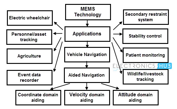
MEMS based devices or sensors are crucial components in various disciplinary areas such as medical equipment, automotive electronics, and portable electronics like computer peripherals, hard drives, cell phones, wireless devices, etc. The commercial applications of MEMS include micro sensors and micro actuators. Some of the specific applications of MEMS technology are discussed below.
Electrical Wheelchairs
For disabled and elderly individuals, electric wheelchairs are important tools. A typical smart wheelchair consists of a standard power wheelchair base to which a computer and a collection of sensors like vision, inertial, etc. along with a seat placed over the base. These sensors are made with MEMS technology and based on these sensors wheelchair navigation systems employs different operating modes.
Personnel Tracking and Navigation
MEMS based inertial sensors are more popular in the field of personnel tracking. In GPS-denied environments, these sensors provide positioning information about the personnel. Such applications include fire fighters inside the building, army personnel tracking, etc. Accelerometers, dead-reckoning sensors and gyroscopes sensors are used for the safety of fire fighters. And in case of army personnel tracking, these sensors are embedded in the shoes or helmets of the personnel.
Agriculture
MEMS based sensors are quite helpful in the precision agriculture. The smart systems are necessary for giving the precise information about the land so that it will be useful in the application of insecticides, fertilizers, land preparation for the crops and harvesting. MEMS based tilt sensors can be used with the GPS system to obtain the roll and pitch estimation for the machinery platform.
Event Data Recorder
Event Data Recorders (EDRs) used in motor vehicles to collect the information such as vehicle acceleration/deceleration data, braking and steering inputs and vehicle system status. In addition, it monitors the speed, brakes and safety systems. The sensors used in the EDR include angular rate sensors, linear accelerometers, triaxial linear accelerometers.
Wildlife and Livestock Tracking
For a continuous positioning and habitual information about the animals, animal tracking system is used with inertial sensors. These tracking units consist of digital cameras for visual aiding of the researches in addition to the inertial dead-reckoning sensors. GPS systems and inertial sensors are integrated with wireless sensor networks which are deployed to monitor the movement of livestock.
Patient Monitoring
MEMS-based sensors are very popular in medical applications and patient monitoring. These sensors are well suited to monitor epilepsy as they can be used to quantify the frequency, intensity and duration of the movements. In addition, MEMS accelerometers are used to detect the falling by high-risk or elderly patients who lose control.
Electronic Stability Control
Generally, electronic stability control is equipped for all new vehicles. MEMS based gyroscope and accelerometers can detect the skidding or loss of control by comparing the vehicle’s actual motion with the steering angle.
Secondary Restraint System
This system is also employed for vehicles. A supplemental (secondary) restraint system (SRS) consists of a deceleration or acceleration sensor which causes airbags to be deployed in the case of a frontal collision. This type of systems sensor modules consists of MEMS accelerometer with a microprocessor.
Vehicle Navigation
For accurate land vehicle based surveying or navigation system needs a high internal navigation system with GPS. But these are limited due to a significant size and high cost. Low cost MEMS inertial sensors made to produce small, light weight, less power and low cost chip-based sensors are reliable for the land vehicle navigation and tracking systems.
Different MEMS Sensors
A sensor that is manufactured using microfabrication and micro machining techniques or simply nothing but a MEMS technology is called as MEMS sensors or micro sensors. Most of the MEMS devices are falling into the sensor class. With the invention of MEMS sensors cause to replace more costly and cumbersome products that are made from assemble parts as in case of pressure sensors. Also, motion detection and measurement becomes easier and very accurate with MEMS accelerometers, which are more popularly used as crash sensors for air bag systems. The following are some of commonly used MEMS sensors which are used in different applications.
MEMS Accelerometers
These are used to measure the static or dynamic force of acceleration. The major categories of accelerometers include silicon capacitive, piezo-resistive and thermal accelerometers. In case of piezo-electric effect, a voltage generated corresponds to the accelerative forces which are acting on microscopic crystal structures on the sensor. Capacitive sensors are designed to operate by generating the electrostatic field and detecting the changes in the field caused when the object or target approaching the sensing area. In case of thermal MEMS sensors a large number of tiny thermocouples are connected in series. Nowadays, MEMS accelerometers widely incorporated in so many electronic portable devices such as media players, cam recorders, gaming devices, etc. In Smart phones these sensors are used to transit between landscape and portrait modes, image stabilizing, anti-blur capturing, pocket mode operation, etc. High standard accelerometers are used for detecting car crashes and to deploy the air bags at just the right time. In addition, these are found in control and monitoring of aerospace and military system applications.
MEMS Gyroscopes
MEMS gyroscopes are used to detect and measure the angular rate of an object. These are works on the principle of vibrating objects undergoing rotation. These are very tiny sensors in which a small resonating mass is shifted as the angular velocity changes when the gyro is rotated. Further, this movement is converted into low current signals. Similar to the accelerometers these sensors also work on different sensing principles like silicon capacitive, piezo-resistive, etc. Some of the types of MEMS gyroscopes include tuning fork, resonant solids, vibrating wheels, vibrating plate gyroscopes. These are integral part of aeronautical control systems since the navigation system requires altitude and rotational rates. In military applications these are used for missile navigation, guidance and smart munitions. In automobiles, MEMS gyros are used for vehicle stability control with steering wheel sensor and rollover detection. And in consumer applications, these are used in input device control of computers and cam recorder stabilization.
MEMS Pressure Sensors
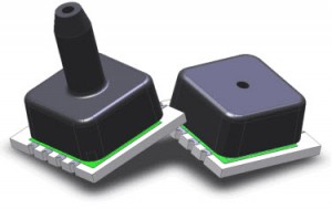
MEMS pressure sensors measure the pressure difference across a silicon diaphragm. Three types of pressure measurements like gauge, absolute and differential pressure are possible with these sensors. In these sensor design, diaphragm is etched from silicon using micro machining process and the measurement techniques include piezo-resistive and capacitive technologies. This sensor is integrated with diaphragm and a set of resistors on integrated chips so that a pressure is detected as a change in resistance when the membrane flexes. These are used in automotive, industrial, medical, process control, defence and aerospace applications. Especially in automotive systems these are used in various applications such as tire pressure monitoring systems, oil pressure sensing, fuel tank vapour pressure, vacuum brake booster, exhaust gas recirculation, engine management system, crash detection, etc. Other types of MEMS devices or sensors includes IR sensors, geomagnetic sensors, microphones, optical devices, RF MEMS, humidity sensors, micro spectrometer, phase shifters, cantilever sensors, etc.
MEMS Magnetic Field Sensor
Magnetic field sensors widely used to measure the magnetic fields and applications of such sensors include position sensing, current detection, speed detection, vehicle detection, geophysical prospecting, space exploration, etc. A new class of magnetic sensors is developed by MEMS technology. MEMS based magnetic sensor detects the magnetic field vector by measuring the amplitude of a mechanical Lorenz force. This MEMS device consists of a current loop on an SiO2 plate and the amplitude of force is detected with a polysilicon piezo resistor Wheatstone bridge. The sensing of mechanical motion of a micro structure can be carried either optically or electronically. In electronic detection method, electrostatic induction and piezo-resistive methods are used. In optical detection, displacement measurement with laser source or LED source is used.
Resonant Magnetic Sensor
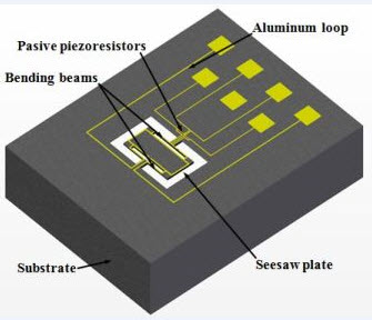
This type of magnetic sensors can detect the magnetic fields with a sensitivity up to 1T and also has 1nT maximum achievable resolution. These sensors are based on Lorenz force of resonating micro machined structures. The structures used in resonant sensors are integrated by clamped – clamped / clamped-free beams, flexion/torsion plates or an array of them. These structures are excited at their resonant frequencies by Lorenz forces or electrostatic forces. This force increases or alters the displacement of a resonant structure; further, this can be measured with piezo-resistive, optical and capacitive sensing techniques. These devices are fabricated using MEMS technology and are in small size that consists of integration of electronic and mechanical components on a single chip. Such MEMS resonant magnetic field sensors are able to give an amplified response if an excitation source applied with a frequency equal to the resonant frequencies or vibrating modes of the structures. The above figure shows the design of resonant magnetic field micro sensor with a highlight on the plate beam structure. In the above figure, an aluminium rectangular loop which is deposited on the silicon plate is the major element of this sensor. The structure is made by the two clamped-free micro beams which are connected to a silicon substrate. For piezo-resistances are connected to a Wheatstone bridge in which two are active that are placed on the micro beams and other two are passive piezo-resistors that are deposited on the substrate. The passive piezo-resistors have fixed-value resistances whereas the active piezo-resistors can shift their resistance magnitudes. Thus, when a Lorenz force causes a see saw motion on the micro plate and the bending of micro beams, two active piezo-resistors change their resistance values. This change in resistance produces a voltage at the output of a Wheatstone bridge. Hence the magnitude of the external magnetic field is measured through the output voltage of the Wheatstone bridge. These MEMS based resonant sensors can be implemented with optical sensing and capacitive sensing techniques. The resonant sensors with optical readout not only reduce their circuitry and weight but increase the immunity to EMI. However, these require complex fabrication processes and also present the problems due to the intrinsic losses of the intrinsic losses of the structural imperfections of the sensors. In case of capacitive sensing, these sensors suffer from parasitic capacitances in the connecting leads that complicate the signal measurements.
Fluxgate sensors
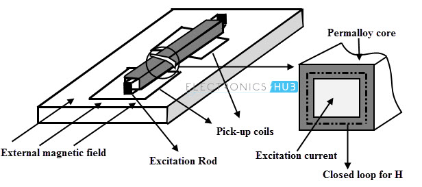
Fluxgate sensors are used for measuring DC or low frequency AC magnetic fields and compared with other magnetic sensors these possesses many advantages like high resolution and ultra high sensitivity. Compared with traditional fluxgate sensors, MEMS based Micro flux gate sensors has advanced features like smaller size, less power consumption, batch production, better performance, and so on. These are used in many applications such as space research, geophysics, mineral prospecting, automation, industrial process control, scientific research, etc. The principle of a fluxgate sensor is based on the external magnetic field dependant periodical saturation of the ferromagnetic material. When a ferromagnetic material surrounded by an exciting coil (that provides AC exciting current) is immersed in a magnetic field, then this current periodically saturates the magnetic material of the core at a frequency twice the excitation frequency. This second harmonic of the output can be measured by using a lock-in technique and is proportional to the external field for a certain field range.
The above figure shows the MEMS based orthogonal fluxgate sensor design reported by Zorlu et al in 2007. According to this, fluxgate sensor is based on micro machined orthogonal type planar structure formed by a perm alloy layer electro deposited on a rectangular copper conductor. With this sensor, the core only 1 mm in length and the sensor has two flat 60 turn pick up coils. Comment * Name * Email * Website
Δ



![]()


![]()