Introduction
One of the main advantages of LEDs over traditional light bulbs is that an LED can be easily controlled i.e. we can easily change its intensity. You might have already used light dimmers but this LED Lamp Dimmer Circuit is a very simple circuit where a bunch of LEDs continuously change its intensity. By making slight modification with respect to the power dissipation, you can even implement this circuit with high-power LEDs for real-time use.
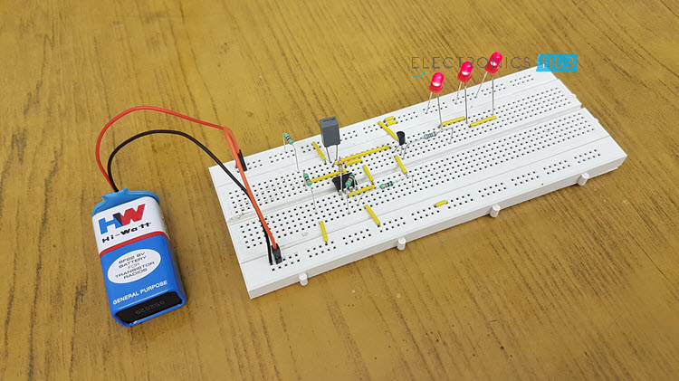
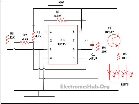
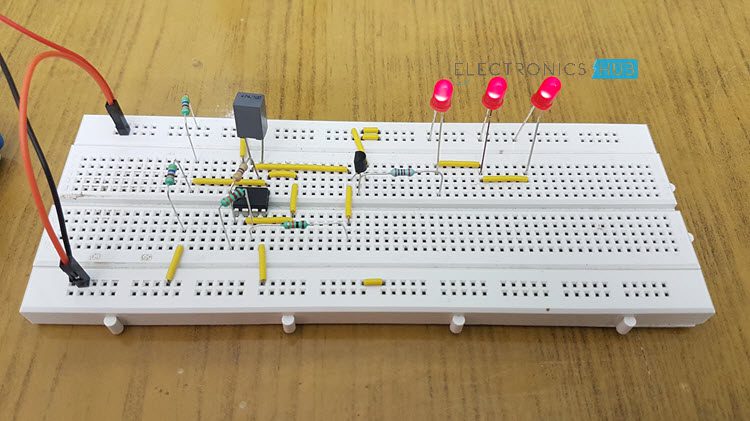
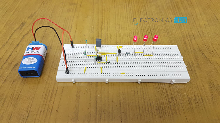
LED Lamp Dimmer Circuit Diagram
Circuit Components
IC LM358 (IC1) – 1 Transistor BC547 (T1) – 1 Resistors (R1, R2) 4.7KΩ – 2 Resistor (R3) 22KΩ – 1 Resistor (R4) 10KΩ – 1 Resistor (R5) 4.7MΩ – 1 Resistor (R6) 100Ω – 1 Capacitor (C1) 0.47µF – 1 LEDs – 3 9V Battery Breadboard Connecting Wires
Component Description
LM358 This IC consists of two independent, high-gain, frequency-compensated operational amplifiers designed to operate from a single supply over a wide range of voltages. Operation from split supplies also is possible if the difference between the two supplies is 3 V to 32 V (3 V to 26 V for the LM2904), and Vcc is at least 1.5 V more positive than the input common-mode voltage. The low supply-current drain is independent of the magnitude of the supply voltage. Transistor A three terminal electronic device employed to amplify weak input signals. A transistor made up of two PN junction diode linked back to back. Transistor are of many type viz bipolar junction transistor, Field effect transistor and photo transistor. They are mainly used in electrical machine as of their lesser size as well as light weight. LED LED stands for Light Emitting Diode. It is made up of semiconductor device. When power supply is provided to LED, electrons combines with the holes and energy is released in the form of light. LED are available in many colors like Red, Orange, Amber, Yellow, Green, Blue and White. Now-a-days, LED’s are available in visible, ultraviolet and infrared wavelengths and have high brightness.
Working of LED Lamp Dimmer Circuit
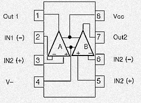
LM358 is mainly made up of a package which contains two independent operational amplifiers of high gain. The most significant attribute of this IC is that we need not provide independent power supply for the functioning of each comparator till the large range of the power supply. LM358 can be employed like transducer amplifier or can be worked as DC gain block etc. The DC voltage gain of the LM358 IC is huge i.e. 100db. Coming to the power supply, this IC can work on the voltage range of 3V to 32V while for the twin power supply this IC work on the range of ±1. 5V to ±16V. And moreover large output voltage is also supported by it. Pin configuration of the IC LM358 is being described below. To get a triangle wave an op-amp is used in the circuit that has been explained here. It is only due to the triangular wave that the LED starts glowing slowly and became brighter and then slowly gets off and again it becomes brighter slowly. The same cycle goes on repeat many of the times. In each independent op-amp of the package, there are two input pins and one pin as the output, as it shown on the figure above. Pin 2, which is a negative pin and pin 3, which is the positive pin are the two input terminals of the op-amp. For the positive feedback pin 3 is used and if there is a desire of the negative feedback pin 2 is used. When there is no feedback given to the op-amp than at that state infinite gain, is the ideal condition for the op-amp.
When the voltage at pin number 2, which is a negative input pin, is higher when compared with the voltage at pin 3 i.e. a positive pin, then the output will be received towards maximum positive voltage while if there is a slight boost at the negative pin of the op-amp as compared with the positive pin of the op-amp than the output moves in the direction of the negative maximum. This characteristic of op-amp craft it appropriate for the use of level detection. The voltage level which we want to detect is applied to either of the input pins and the voltage to be detected is applied to the other pin. In our circuit, we are applying a voltage on positive pin that is at pin 3 and voltage to be detected is applied at negative pin. At the instance when the input voltage given to the positive pin is a little more than that of the voltage given at the negative pin, at that condition the output rapidly mounts to the positive maximum and reside in the positive state till the input voltage drop lower than the level to be detected. The same phenomenon is being used in this circuit too. For the timing component resistor R5 as well as capacitor C1 is used. State of the pin 3 switches from high to low condition depending upon the charging and discharging of the capacitor used in the circuit and as a reference to it pin 2 of the op-amp obtains the desire output. For the driving of the LED transistor T1 is used in the circuit as a signal amplifier and to protect the LED from the damage due to high current resistor R6 is employed in the circuit as a current limiter. Comment * Name * Email * Website
Δ
![]()
![]()
![]()
![]()
![]()

